- 您现在的位置:买卖IC网 > Sheet目录2006 > LTC2642IDD-16#PBF (Linear Technology)IC DAC 16BIT VOUT 10-DFN
LTC2641/LTC2642
5
26412fc
For more information www.linear.com/LTC2641
Note 1: Stresses beyond those listed under Absolute Maximum Ratings
may cause permanent damage to the device. Exposure to any Absolute
Maximum Rating condition for extended periods may affect device
reliability and lifetime.
Note 2: Continuous operation above the specified maximum operating
junction temperature may impair device reliability.
Note 3: LTC2641-16/LTC2642-16 ±1LSB = ±0.0015% = ±15.3ppm of full
scale. LTC2641-14/LTC2642-14 ±1LSB = ±0.006% = ±61ppm of full scale.
LTC2641-12/LTC2642-12 ±1LSB = ±0.024% = ±244ppm of full scale.
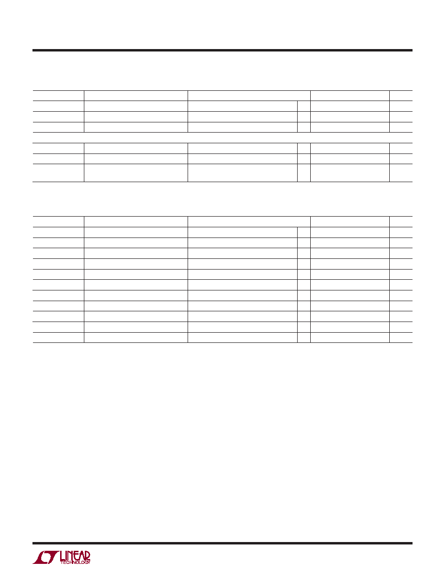
elecTrical characTerisTics The
l
denotes the specifications which apply over the full operating
temperature range, otherwise specifications are at TA = 25°C. VDD = 3V or 5V, VREF = 2.5V, CL = 10pF, GND = 0, RL = ∞unless otherwise
specified.
SYMBOL
PARAMETER
CONDITIONS
MIN
TYP
MAX
UNITS
IIN
Digital Input Current
VIN = GND to VDD
l
±1
A
CIN
Digital Input Capacitance
(Note 6)
l
3
10
pF
VH
Hysteresis Voltage
0.15
V
Power Supply
VDD
Supply Voltage
l
2.7
5.5
V
IDD
Supply Current, VDD
Digital Inputs = 0V or VDD
l
120
200
A
PD
Power Dissipation
Digital Inputs = 0V or VDD, VDD = 5V
Digital Inputs = 0V or VDD, VDD = 3V
0.60
0.36
mW
TiMing characTerisTics The
l
denotes the specifications which apply over the full operating temperature
range, otherwise specifications are at TA = 25°C. VDD = 3V or 5V, VREF = 2.5V, CL = 10pF, GND = 0, RL = ∞unless otherwise specified.
SYMBOL
PARAMETER
CONDITIONS
MIN
TYP
MAX
UNITS
t1
DIN Valid to SCLK Setup Time
l
10
ns
t2
DIN Valid to SCLK Hold Time
l
0
ns
t3
SCLK Pulse Width High
l
9
ns
t4
SCLK Pulse Width Low
l
9
ns
t5
CS Pulse High Width
l
10
ns
t6
LSB SCLK High to CS High
l
8
ns
t7
CS Low to SCLK High
l
8
ns
t8
CS High to SCLK Positive Edge
l
8
ns
t9
CLR Pulse Width Low
l
15
ns
fSCLK
SCLK Frequency
50% Duty Cycle
l
50
MHz
VDD High to CS Low (Power-Up Delay)
30
s
Note 4: ROUT tolerance is typically ±20%.
Note 5: Reference input resistance is code dependent. Minimum is at
871Chex (34,588) in unipolar mode and at 671Chex (26, 396) in bipolar
mode.
Note 6: Guaranteed by design and not production tested.
Note 7: Guaranteed by gain error and offset error testing, not production
tested.
发布紧急采购,3分钟左右您将得到回复。
相关PDF资料
LTC2704IGW-16#PBF
IC DAC 16BIT QUAD VOUT 44-SSOP
LTC2751AIUHF-16#PBF
IC DAC 16BIT CUR OUT 38-QFN
LTC2752ACLX#PBF
IC DAC 16BIT DUAL CUR OUT 48LQFP
LTC2753AIUK-16#TRPBF
IC DAC 16BIT DUAL 48-QFN
LTC2754AIUKG-16#PBF
IC DAC 16BIT QUAD IOUT 52-QFN
LTC2755AIUP-16#PBF
IC DAC 16BIT CUR OUT 64-QFN
LTC2757ACLX#PBF
IC DAC 18BIT PAR 48LQFP
LTC2758AILX#PBF
IC DAC 18BIT SPI/SRL 48-LQFP
相关代理商/技术参数
LTC2642IDD-16#TRPBF
功能描述:IC DAC 16BIT VOUT 10-DFN RoHS:是 类别:集成电路 (IC) >> 数据采集 - 数模转换器 系列:- 标准包装:47 系列:- 设置时间:2µs 位数:14 数据接口:并联 转换器数目:1 电压电源:单电源 功率耗散(最大):55µW 工作温度:-40°C ~ 85°C 安装类型:表面贴装 封装/外壳:28-SSOP(0.209",5.30mm 宽) 供应商设备封装:28-SSOP 包装:管件 输出数目和类型:1 电流,单极;1 电流,双极 采样率(每秒):*
LTC2642IMS-12#PBF
功能描述:IC DAC 12BIT VOUT 10-MSOP RoHS:是 类别:集成电路 (IC) >> 数据采集 - 数模转换器 系列:- 产品培训模块:LTC263x 12-, 10-, and 8-Bit VOUT DAC Family 特色产品:LTC2636 - Octal 12-/10-/8-Bit SPI VOUT DACs with 10ppm/°C Reference 标准包装:91 系列:- 设置时间:4µs 位数:10 数据接口:MICROWIRE?,串行,SPI? 转换器数目:8 电压电源:单电源 功率耗散(最大):2.7mW 工作温度:-40°C ~ 85°C 安装类型:表面贴装 封装/外壳:14-WFDFN 裸露焊盘 供应商设备封装:14-DFN-EP(4x3) 包装:管件 输出数目和类型:8 电压,单极 采样率(每秒):*
LTC2642IMS-12#TRPBF
功能描述:IC DAC 12BIT VOUT 10-MSOP RoHS:是 类别:集成电路 (IC) >> 数据采集 - 数模转换器 系列:- 产品培训模块:LTC263x 12-, 10-, and 8-Bit VOUT DAC Family 特色产品:LTC2636 - Octal 12-/10-/8-Bit SPI VOUT DACs with 10ppm/°C Reference 标准包装:91 系列:- 设置时间:4µs 位数:10 数据接口:MICROWIRE?,串行,SPI? 转换器数目:8 电压电源:单电源 功率耗散(最大):2.7mW 工作温度:-40°C ~ 85°C 安装类型:表面贴装 封装/外壳:14-WFDFN 裸露焊盘 供应商设备封装:14-DFN-EP(4x3) 包装:管件 输出数目和类型:8 电压,单极 采样率(每秒):*
LTC2642IMS-14#PBF
功能描述:IC DAC 14BIT VOUT 10-MSOP RoHS:是 类别:集成电路 (IC) >> 数据采集 - 数模转换器 系列:- 标准包装:47 系列:- 设置时间:2µs 位数:14 数据接口:并联 转换器数目:1 电压电源:单电源 功率耗散(最大):55µW 工作温度:-40°C ~ 85°C 安装类型:表面贴装 封装/外壳:28-SSOP(0.209",5.30mm 宽) 供应商设备封装:28-SSOP 包装:管件 输出数目和类型:1 电流,单极;1 电流,双极 采样率(每秒):*
LTC2642IMS-14#TRPBF
功能描述:IC DAC 14BIT VOUT 10-MSOP RoHS:是 类别:集成电路 (IC) >> 数据采集 - 数模转换器 系列:- 标准包装:47 系列:- 设置时间:2µs 位数:14 数据接口:并联 转换器数目:1 电压电源:单电源 功率耗散(最大):55µW 工作温度:-40°C ~ 85°C 安装类型:表面贴装 封装/外壳:28-SSOP(0.209",5.30mm 宽) 供应商设备封装:28-SSOP 包装:管件 输出数目和类型:1 电流,单极;1 电流,双极 采样率(每秒):*
LTC2642IMS-16#PBF
功能描述:IC DAC 16BIT VOUT 10-MSOP RoHS:是 类别:集成电路 (IC) >> 数据采集 - 数模转换器 系列:- 标准包装:1 系列:- 设置时间:4.5µs 位数:12 数据接口:串行,SPI? 转换器数目:1 电压电源:单电源 功率耗散(最大):- 工作温度:-40°C ~ 125°C 安装类型:表面贴装 封装/外壳:8-SOIC(0.154",3.90mm 宽) 供应商设备封装:8-SOICN 包装:剪切带 (CT) 输出数目和类型:1 电压,单极;1 电压,双极 采样率(每秒):* 其它名称:MCP4921T-E/SNCTMCP4921T-E/SNRCTMCP4921T-E/SNRCT-ND
LTC2642IMS-16#TRPBF
功能描述:IC DAC 16BIT VOUT 10-MSOP RoHS:是 类别:集成电路 (IC) >> 数据采集 - 数模转换器 系列:- 标准包装:47 系列:- 设置时间:2µs 位数:14 数据接口:并联 转换器数目:1 电压电源:单电源 功率耗散(最大):55µW 工作温度:-40°C ~ 85°C 安装类型:表面贴装 封装/外壳:28-SSOP(0.209",5.30mm 宽) 供应商设备封装:28-SSOP 包装:管件 输出数目和类型:1 电流,单极;1 电流,双极 采样率(每秒):*
LTC-2651TBE-01
制造商:LITEON 功能描述:8*4 ND, 0.28 inch, common anode, color-blue